Technology
Alba Scientific specialises in advanced deposition systems, quantum technologies and life sciences research tools. Our portfolio includes advanced physical vapour deposition (PVD) systems, ultra-high vacuum (UHV) components, atomic force microscopy (AFM) and quantum sensing instruments that empower breakthroughs across industries such as nanotechnology, materials science, life sciences and quantum computing. Designed for research labs, academic institutions and industrial applications, our technologies offer precision, reliability and flexibility to support the future of science and innovation.
Our core technologies and their impact on key industries
Magnetron sputtering deposition
Magnetron sputtering is a physical vapour deposition (PVD) technique that uses high-energy ions to dislodge atoms from a target material, depositing them as an ultra-thin film on a substrate. By applying a magnetic field, the process enhances plasma density and deposition efficiency, delivering precise, uniform coatings at the nanoscale. This technology is integral to nanotechnology, materials science and biomedical engineering, enabling advanced surface modifications for improved performance and biocompatibility.
Key features:
• Fully UHV-capable, producing high-purity thin film coatings
• Multi-material coating supporting metals, alloys and ceramics
• Robust, reliable performance engineered for the needs of research labs
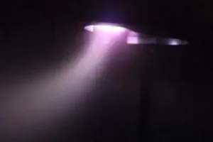
Image credit: Co-deposit up to 3 materials from one UHV source, Nikalyte.
Applications:
• Nanoparticle and quantum dot fabrication for imaging and diagnostics
• Biosensor development for rapid, sensitive detection
• Drug delivery systems with controlled release profiles
• Biocompatible coatings for implants and medical instruments
• Thin-film electronics and optical devices
E-Beam evaporation
Electron beam evaporation (e-beam evaporation) is a physical vapour deposition (PVD) technique in which a focused high-energy electron beam heats and vaporises a target material. The vapour then condenses onto the substrate, forming a thin film with exceptional purity, uniformity and thickness control. This method is widely used in advanced materials research, nanotechnology and biomedical engineering for creating high-performance coatings and functional nanostructures.
Key features:
- Single power supply that streamlines operation, reduces maintenance and ensures consistent, high-quality deposition
- UHV compatibility that performs in ultra-high vacuum environments for contamination-free thin films
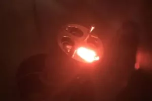
Image credit: Co-evaporation of up to 4 materials, Nikalyte.
Applications:
- Advanced materials and thin-film research
- Semiconductor and photonic device fabrication
- Energy technologies: solar cells, battery electrodes
- Biomedical coatings for implants and devices
- Biosensors for diagnostics and monitoring
Nanoparticle deposition systems
Nanoparticle deposition using the terminated gas condensation (TGC) technique involves generating nanoparticles in a controlled gas environment, where vapourised atoms or molecules condense into particles before being deposited onto a substrate. This method offers precise control over particle size, distribution and morphology, enabling the creation of custom-engineered nanomaterials for targeted biomedical and nanotechnology applications.
Key features:
- Customisable particle size, tailoring nanoparticles to specific diameters
- UHV-ready deposition, maintaining a contamination-free environment
- High-precision dispersion, achieving uniform nanoparticle distribution
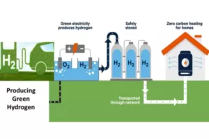
Image credit: Nanoparticle catalysts for green hydrogen, Nikalyte.
Applications:
- Nanomaterial-based cancer therapies
- Biomedical implants with enhanced biocompatibility
- Catalysis and chemical reaction enhancement
- Sensors for medical, environmental and industrial use
Ultra-high vacuum (UHV) technology
Ultra-high vacuum (UHV) technology refers to the creation and maintenance of extremely low pressures, typically below 10^-9 mbar, essential for minimising contamination in high-precision experiments. UHV environments are crucial for surface science, nanotechnology and materials science, where clean, controlled conditions are needed for reliable results.
Key features:
- Achieves ultra-low pressure (down to 10^-12 mbar)
- Prevents contamination by minimising exposure to air and moisture
- Highly stable and reliable performance for long-term research
- Modular components such as feedthroughs, motion control systems and coaxial cables for tailored solutions
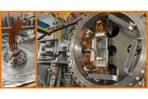
Image credit: CARME vacuum chamber, UKRI STFC project, at STFC Daresbury Laboratory. Flanges by Allectra.
Applications:
- Semiconductor fabrication for chip manufacturing and thin-film deposition
- Surface analysis enabling XPS and STM for material characterisation
- Supporting the development of nanoelectronics and photonic devices
- Providing clean environments for high-resolution imaging
Atomic force microscopy (AFM)
Atomic force microscopy is a high-resolution scanning probe technique that maps surfaces at the nanometre and even atomic scale. By measuring the interaction forces between a sharp probe tip and the sample surface, AFM provides 3D surface topography and quantitative force measurements without the need for complex sample preparation. This technology is indispensable in nanotechnology, SEMICON and biomaterials research, offering detailed insights into material properties, microstructure and performance characteristics.
Key features:
- Tailored for all levels, designed for newcomers, students and researchers
- Innovative and modular, offering an open design for easy customisation, enabling innovation
- Affordable and accessible, providing cost-effective solutions for educators and innovators
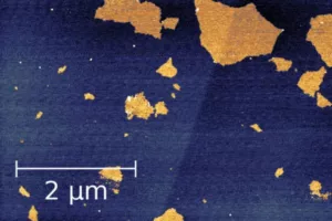
Image credit: Flakes of graphene deposited on mica, AFM workshop.
Applications:
- Assists in nano-patterning and fabrication of semiconductor devices
Mechanical property mapping of semiconductor materials for MEMS.
Biological imaging at the nanoscale
- Analyse polymer surfaces and nanostructures for nanocomposites.
- Characterizes graphene’s surface properties, and defects for nanoelectronics.
Atomic force microscopy (AFM) probes
AFM probes are the exchangeable sensors at the heart of atomic force microscopy. The probe’s cantilever stiffness is typically matched to the measured surface’s stiffness, while the probe’s tip dimensions influence the image resolution and aspect ratio measurable; the probe’s chip is critical for handling. AFM probes are readily available for 3D nanoscale imaging, electrical, magnetic, thermal, and mechanical measurements, as well as a myriad of more niche measurements such as SECM, femtofluidics, etc.
Key features:
- Unique batch processing for highest performance reproducibility
- Conical tip design for simple deconvolution
- Pt-coated electrical probes, more robust coating thanks to novel design
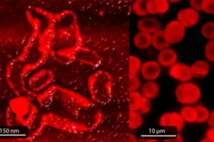
Image credit: Protein imaging in Alzheimer’s blood (left) and red blood cells (right), NuNano.
Applications:
- Surface topography, spectroscopy of soft to hard materials
- Electrical measurements such as C-AFM, EFM, SKPM, PFM, etc.
- Semiconductor inspection, high aspect ratio measurements
- Individually SEM characterised AFM probes
- Bespoke probe engineering
MALDI-TOF mass spectrometry
Matrix-assisted laser desorption/ionisation time-of-flight mass spectrometry (MALDI-TOF MS) is a soft ionisation technique that uses a pulsed laser to desorb and ionise molecules co-crystallised with a UV-absorbing matrix. The resulting ions are separated by their flight time through a field-free drift region, with mass determined by time of arrival at the detector. MALDI-TOF is well established across proteomics, microbiology, polymer science, and clinical diagnostics for its speed, sensitivity, and ability to analyse large, intact biomolecules without fragmentation.
Key features:
- Instrument configurations from compact benchtop linear TOF to high-resolution ToF-ToF research platforms
- Reflectron mode for improved mass resolution and fM-range peptide detection sensitivity
- Imaging and MS/MS capability for spatially resolved analysis and peptide sequencing
Image credit: Powerful polymer analysis, PEG (Polyethylene Glycol sample) showing the chain length distribution, SAI.
Applications:
- Proteomics, peptide mapping, and protein identification
- Clinical microbiology: rapid bacterial identification
- Polymer characterisation and pharmaceutical quality control
Secondary ion mass spectrometry (SIMS)
Secondary ion mass spectrometry (SIMS) is a surface analysis technique in which a focused primary ion beam bombards a sample surface, sputtering secondary ions that are collected and analysed by a mass spectrometer. SIMS provides elemental, isotopic, and molecular information from the outermost atomic layers of a surface, making it uniquely powerful for characterising thin films, coatings, and complex material interfaces. Instrument configurations range from entry-level desktop systems for routine surface monitoring through to high-resolution research platforms capable of sub-micron imaging.
Key features:
- Time-of-flight and quadrupole analyser options supporting all three SIMS operating modes
- Sub-micron spatial resolution with active antivibration and high-resolution primary ion optics
- Full mass range acquisition for retrospective analysis without prior sample assumptions
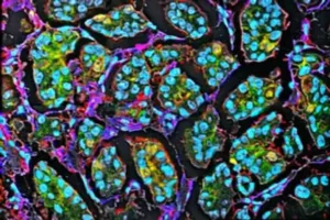
Image credit:Multiplexed ion beam image of breast cancer cells showing six proteins: e-cadherin (green), vimentin (blue), actin (red), estrogen receptor, progesterone receptor, and Ki67. Cells positive for estrogen receptor, progesterone receptor, and Ki67 appear yellow, while those expressing estrogen and progesterone receptors appear aqua, SAI.
Applications:
- Surface and thin-film characterisation in materials science and semiconductors
- Depth profiling, failure analysis, and industrial quality assurance
- Imaging of biological surfaces and tissue sections
Nanoprojectile secondary ion mass spectrometry (NP-SIMS)
Nanoprojectile secondary ion mass spectrometry (NP-SIMS) is a next-generation surface analysis technique in which highly-charged, time-tagged nano-projectiles bombard a sample surface, generating significantly higher secondary ion yields per impact than conventional primary ion beams. Each impact is treated as an independent event, secondary ions are collected separately at 1 kHz, building one million individual mass spectra in 20 minutes. This event-by-event approach eliminates the signal averaging that limits conventional TOF-SIMS, delivering spatially resolved molecular and chemical information from sampling areas as small as 10 nm. Because the surface is sampled stochastically over a 10–200 µm diameter area, the analysis is quasi-non-destructive, leaving the sample available for complementary techniques such as SEM or AFM.
Key features:
- ~10 nm sampling area with event-by-event detection — no signal averaging
- Co-emission correlation of molecular species from each individual impact
- Quasi-nondestructive analysis compatible with SEM, AFM, and downstream techniques
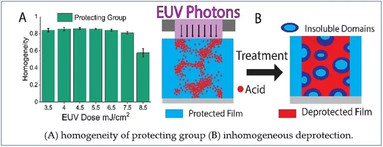
Image credit:Bringing nanoscale molecular insight to EUV resist fabrication. (Adapted from Cruz et al., Journal of Micro/Nanopatterning, Materials,
and Metrology, 2022) Bienne Technology.
Applications:
- Nanoscale chemical mapping in materials science, semiconductors, and thin films
- Molecular imaging of cells, tissue, and biological nanoparticles
- Label-free characterisation in drug delivery, lipidomics, and biomarker research
Superconducting qubits
Superconducting qubits are one of the most promising technologies for quantum computing hardware. Created by nanostructuring a Josephson junction (two superconductors separated by an insulator) on a support chip, these chips need to be cooled to mK temperature and protected from any noise source that could reduce the quantum coherence.
Alba Scientific partners with ConScience AB to offer you their off-the-shelf Qubit-in-a-box, QuiB.
Key features:
- Fixed frequency, tunable, XY sweepable configurations available
- Typical lifetime 130 µs, >200 µs achieved
- Batch or, for a surcharge, individual certification available
- Supplied in a compact Au-plated OFC package with multiple SMPM (QiB1, 2) or SMA (QiB0) connectors
Image credit: Unprecedented tracking of microbial cultures, ConScience.
Applications:
- Cryostat testing, system noise/disturbance reduction
- Benchmarking, metrology
- Teaching, training
- Pharmaceutical research and drug discovery
Nitrogen-vacancy (NV) diamond quantum sensors
Nitrogen-vacancy diamonds are quantum-grade materials with atomic-scale defects that enable ultra-sensitive detection of magnetic, thermal, and electric fields at the nanoscale. Their unique properties make them ideal quantum sensors, and they are used in fields ranging from materials research (e.g. spintronics) to health science (MEG), GPS-free navigation, and even remote, drone-based metal detection. Our NV diamond engineering manufactures surface-close NV in light guides to improve sensitivity and lateral resolution.
Key features:
- Reproducible structures for simple navigation
- Surface-close NV embedding for best lateral resolution
- 5-20x PL enhancement through engineered structures on the diamond
Image credit: Integration of germanium-vacancy single-photon emitter arrays in diamond nanopillars, Qnami Quantum Foundry.
Applications:
- Reference for metrology
- Instrument set-up and optimisation
- Enhanced signals for NV multiplexing
- Improved sensitivity
Surface-enhanced raman spectroscopy (SERS) substrates
SERS substrates leverage surface-enhanced Raman scattering to achieve ultra-sensitive molecular detection, enabling the identification of low-concentration molecules that are undetectable with conventional Raman spectroscopy. By using metallic nanostructures to amplify Raman signals, SERS technology delivers exceptional precision for life sciences, chemical analysis, and biosensing. This makes it a powerful tool for drug testing, cancer detection, and environmental monitoring.
Key features:
- Ag and Au nanoparticle coatings significantly boost Raman signal intensity for trace biomolecule detection
- High surface-to-volume ratio maximises signal enhancement for greater sensitivity and reproducibility
- Versatile application range, suitable for drug testing, cancer research, and biomedical diagnostics
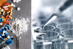
Detection of Narcotics: Includes substances such as Fentanyl, Heroin, and MDMA.
Applications:
- Drug testing and pharmaceutical quality control
- Cancer detection at early stages
- Chemical analysis in research and industry
- Environmental monitoring for pollutants and toxins
- Trace detection for security and forensic applications