
Atomic force microscopy
A sharp probe tip scans across a surface, measuring interaction forces at the nanoscale to produce high-resolution 3D maps of surface topography, mechanical properties and electrical characteristics no vacuum, no staining, no complex sample preparation required.
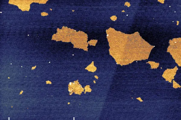
Introduction
Imagine running an extremely fine needle across a surface so lightly that it can detect individual atoms. That is the basic principle behind Atomic Force Microscopy (AFM). AFM uses a tiny probe with a sharp tip that moves across a sample’s surface. As the tip scans the surface, it responds to very small forces between the tip and the material. A laser system measures these movements with exceptional precision. The information collected is used to create a highly detailed 3D image of the surface, revealing tiny features such as bumps, grooves, steps and textures that are far too small to be seen with a conventional microscope.
One of the main advantages of AFM is its versatility. It can be used to examine a wide range of materials, including metals, plastics, semiconductors, biological samples and even living cells. Unlike some microscopy techniques, AFM usually does not require the sample to be coated or placed in a vacuum, allowing materials to be studied in conditions that are closer to their natural state.
Atomic Force Microscopy (AFM) is a scanning probe technique that measures tip–sample interaction forces to generate high-resolution surface topography. A sharp tip mounted on a microfabricated cantilever scans the sample surface, while an optical lever system detects cantilever deflection and provides feedback for image acquisition.
AFM operates in contact, tapping and non-contact modes, enabling the characterisation of a wide range of materials with nanometre-scale lateral resolution and sub-ångström vertical sensitivity. Beyond topographical imaging, advanced AFM techniques can quantify mechanical, electrical, magnetic and chemical properties at the nanoscale.
Atomic Force Microscopy (AFM) measures tip–sample interactions across both attractive and repulsive force regimes. In contact mode, cantilever deflection is related directly to interaction force through Hooke’s law, while non-contact and tapping modes detect changes in cantilever dynamics arising from force gradients. Dynamic techniques such as AM-AFM and FM-AFM provide enhanced sensitivity to tip–sample interactions, with FM-AFM capable of atomic-resolution imaging under ultra-high vacuum conditions.
Force–distance curves can be used to determine elastic modulus, adhesion and viscoelastic behaviour, while advanced modes including KPFM, MFM, EFM and c-AFM enable nanoscale electrical, magnetic and conductivity mapping.
Atomic Force Microscopy (AFM) is widely used in chemistry to study surfaces and interfaces at the nanoscale under ambient or liquid conditions. It provides detailed information on surface topography, roughness and morphology across thin films, polymers, coatings and nanoparticle systems. AFM can also measure adhesion, surface forces and mechanical properties, making it valuable for investigating molecular interactions, material performance and surface behaviour. In electrochemical studies, liquid-cell AFM enables real-time observation of corrosion, film growth and surface changes in working environments.
Atomic Force Microscopy (AFM) enables high-resolution imaging of biological samples, including cells, proteins, DNA and membranes, in their natural hydrated environment without the need for staining or fixation. This allows researchers to observe living cells in real time and monitor changes caused by drugs, environmental conditions or mechanical stimulation. AFM can also measure the mechanical properties of individual cells and investigate interactions between biological molecules, providing valuable insights for disease research, drug development and diagnostics. In addition, AFM can reveal detailed surface features of viruses and protein assemblies at the nanoscale.
Key features
Areas of use
AFM is used any time a researcher needs to see or measure something at the nanoscale that other techniques cannot access:
- Checking the surface roughness of a semiconductor wafer before depositing a coating
- Imaging protein molecules or DNA strands on a surface
- Measuring how stiff or soft a biological cell is
- Mapping the texture of a polymer film to understand how it will perform
- Counting the number of layers in a graphene sample
- Investigating the surface of a battery electrode after charging and discharging
- Semiconductors and MEMS : Surface roughness, step height and grain structure analysis of thin films; nanomechanical characterisation of MEMS device layers; electrical property mapping using Conductive AFM (c-AFM) and Scanning Kelvin Probe Microscopy (SKPM).
- 2D Materials : Layer thickness measurement, defect mapping and interlayer force analysis in graphene, MoS₂ and hBN; characterisation of stacking order and moiré structures.
- Polymer Science : Phase imaging and nanomechanical mapping of polymer blends, block copolymers and nanocomposites; adhesion and surface energy characterisation.
- Biology and Biomedicine : Cell mechanics, membrane imaging in liquid environments, single-molecule interaction studies and virus particle characterisation.
- Electrochemistry : In-situ imaging of electrode surfaces during electrochemical cycling; monitoring of corrosion processes and film growth.
- Tribology and Coatings : Friction force measurements, wear analysis and thin-film adhesion characterisation.
- Quantum Materials : Atomic-resolution imaging of surface reconstructions, charge density waves and moiré superlattices under ultra-high vacuum (UHV) conditions; non-contact AFM (nc-AFM) imaging of reactive surfaces where STM has limitations.
- Mechanical Resonators :Characterisation of nanoelectromechanical systems (NEMS), including cantilever and membrane devices; stiffness and quality factor (Q-factor) mapping.
- Magnetic Nanostructures :Magnetic Force Microscopy (MFM) imaging of domain walls, skyrmions and vortex states in magnetic thin films and nanostructured materials.
- Surface Potential Mapping : Kelvin Probe Force Microscopy (KPFM) analysis of work function variations, contact potential differences and charge trapping in semiconductor devices and heterostructures.
- Nanoscale Heat Transport : Scanning Thermal Microscopy (SThM) for local thermal conductivity measurements and heat transport analysis at the nanoscale.
- Self-Assembled Monolayers : Characterisation of domain structure, packing defects and molecular organisation on gold, mica and oxide surfaces.
- Nanoparticle Characterisation : Analysis of particle size distribution, aggregation behaviour and surface morphology in colloidal systems and deposited nanoparticles.
- Polymer Surfaces : Surface roughness analysis, phase separation studies and nanomechanical mapping of polymer blends and block copolymers.
- Catalytic Surfaces : Nanoscale imaging of surface structure, active sites and surface restructuring during catalytic processes using in-situ liquid AFM.
- Crystal Growth : Investigation of step-flow dynamics, nucleation processes and crystal growth kinetics at solid–liquid interfaces.
- Cell Mechanics : Young’s modulus mapping of live cells in buffer solutions; investigation of stiffness changes associated with cancer, infection and drug response.
- Membrane Biophysics : High-resolution imaging of lipid bilayers, membrane proteins and supported lipid bilayers in liquid environments.
- Single-Molecule Force Spectroscopy : Measurement of receptor–ligand interactions, protein unfolding behaviour and the mechanical properties of DNA.
- Microbiology : Imaging of bacterial cell walls, biofilm architecture and surface structures, including pili and flagella, under native conditions.
- Virology : Characterisation of the surface topography and mechanical properties of individual virus particles, including capsid deformation and rupture behaviour.
Application areas
Deep reading
- Atomic Force Microscopy Peter Eaton & Paul West —foundational reading
- A Beginner’s Guide to AFM Probing for Cell Mechanics
- Top AFM Papers of 2025 — NuNano (current research)
- AFM Tutorials — Fundamentals Explained
- AFM for Cross-Disciplinary Materials Research
- 12 brilliant books on AFM
- Soft Matter Analysis via AFM — A Review