

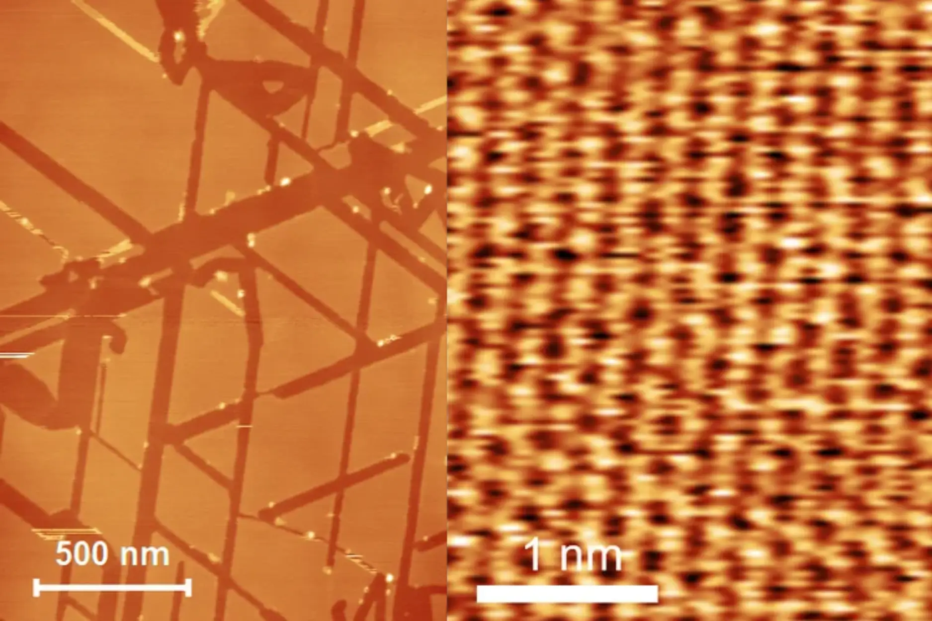
Lattice-resolution AFM image of hexagonal boron nitride taken with a NuNano SCOUT 70 RAl probe
NuNano SCOUT and SPARK AFM probes have helped researchers at the University of Nottingham resolve the hBN lattice, measure etch tracks one atomic layer deep and map conductive pathways in graphene nanoribbons. Read offline
The demand for faster, smaller and cheaper electronics shows no sign of slowing. Conventional semiconductor materials and processes have their limits, so researchers are looking for new materials that can be built into devices at the nanoscale.
Graphene and hexagonal boron nitride (hBN) are two of the most promising. Graphene conducts and hBN insulates, which makes them a natural pairing for circuitry only a few atoms thick. The challenge is controlling how the two come together, and seeing what has happened at each step.
Professor Peter Beton and his team at the University of Nottingham have been working on exactly that. Atomic force microscopy (AFM) has been central to their work, and for the last seven years they have relied on NuNano probes to do it.
How the graphene nanoribbons were grown
The team’s approach uses hBN as a template. First, nickel nanoparticles were deposited onto hBN flakes by thermal evaporation and annealed in a mixture of hydrogen and argon. As they heated, the nanoparticles moved along the crystal’s zigzag lattice directions, etching oriented trenches into the top layer of the flake. The nickel was then removed with a wet chemical etch, leaving the trenches behind. Graphene nanoribbons (GNRs) were grown into them by high-temperature molecular beam epitaxy (HT-MBE), with the trenches acting as a blueprint for their growth. Each of these steps changes the surface at the atomic scale, so the team used AFM to characterise the samples at every stage of preparation and growth.Lattice-resolution AFM with SCOUT 70 RAl
For topographic imaging, the group used NuNano SCOUT 70 RAl silicon probes. After the nickel was removed, AFM showed the etch tracks clearly. Some were very shallow, at 0.36 nm, or roughly one atomic layer. Others reached 1.1 nm, around three layers. Most were just one layer deep. The probes also resolved the hBN lattice itself, with sub-nanometre resolution. Professor Beton describes the SCOUT 70 RAl as part of a “highly reliable combination” that lets his group readily achieve lattice resolution on hBN and the other 2D materials they study. That level of detail let the team follow the early growth of the nanoribbons. They found that at high growth temperatures, the GNR growth rate affected whether the templating hBN step was terminated with boron or nitrogen atoms.Conductive AFM with SPARK 70 Pt
Knowing what the nanoribbons look like is only half the picture. For electronics, what matters is how they conduct. To study the electrical performance of the fully grown GNRs, the team switched to NuNano SPARK 70 Pt conductive probes and carried out conductive AFM (cAFM). The measurements revealed a conductive network forming within the hBN surface. They also showed signs of electrons moving between different sublattices at the interface between graphene and hBN, an effect known as intervalley scattering. Research Fellow Dr Jonathan Bradford reports that the SPARK probes achieved lattice resolution in cAFM mode, despite challenging sample conditions.What this means for 2D materials research
AFM gave the Nottingham group both the topography and the electrical behaviour of their graphene nanoribbons at the nanoscale. Together, these results improved their understanding of how the graphene and hBN interface forms, and of how the material could be used in extremely thin electronic devices and circuits. For anyone working with 2D materials, the study shows what the right AFM probes make possible: lattice resolution on hBN, step heights of a single atomic layer, and conductive measurements at the same scale.Reference
Bradford, J., Cheng, T. S., James, T. S. S., Khlobystov, A. N., Mellor, C. J., Watanabe, K., Taniguchi, T., Novikov, S. V., & Beton, P. H. (2023). Graphene nanoribbons with hBN passivated edges grown by high-temperature molecular beam epitaxy. 2D Materials, 10, 035035. Read full paper hereAlba Scientific supplies NuNano AFM probes to researchers across the Benelux, DACH and Italy, backed by local application expertise and technical support. Get in touch to find the right probe for your 2D materials research.
Follow us on linkedin